
| Mr. Fixit's PC Upgrade and Repair |
| System Memory 101 |

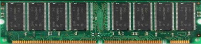
168-pin DIMM SDRAM
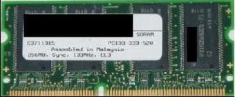
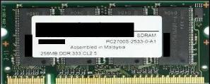
144-pin SO-DIMM SDRAM
With the introduction to Double Data Rate (DDR) SDRAM in 2000, the original SDRAM modules
were referred to as Single Data Rate (SDR) SDRAM because the modules only transferred data
on the RISE of the clock pulse. DDR memory can transfer data on the RISE and FALL of the
clock pulse, doubling data transfers. Today, DDR achieved a maximum clock speed of 266MHz,
but because data can now be transferred on the rise and fall of the clock pulse, the bus speed is
doubled to 533 million transfers per second (266 x 2) or 4,266MB/s. DDR modules are classified
as DDR-###, that identifies the module's million transfers per second (MT/s) bus speed and the
PC-#### that refers to the amount of data transferred per second (MB/s). DDR memory found
their way into Graphics cards and didn't catch the mainstream till 2001. The clock speed (MHz)
is the Bus speed divided by 2. The Clock and Bus speeds are not to be confused.
184-pin DDR DIMM SDRAM
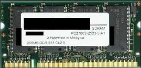
200-pin DDR SO-DIMM SDRAM
|
In 2004, DDR2 hit the market with improved performance over the DDR, reaching 8,000MB/s at a 500MHz clock speed. This was possible by using
differential signaling making the modules immune to noise and 'cross-talk' interference. "Differential signaling" refers to how data is transfered and is very
much like how SATA drives transfer data. Each data pathway has 2 wires that are paired. When data is sent/received, one wire is postive and the paired wire
is negative of the same voltage as the postive wire. For example if 1 wire is +5V then the paired wired has to be -5V. An added bonus was the voltage
requirment. DDR memory used 2.5V, but with DDR2 memory the voltage dropped to 1.8V allowing the modules to consume less energy and produce less
heat. DDR2 was also redesigned to double the internal data bandwidth.
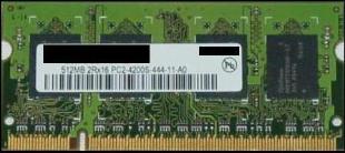
240-pin DDR2 DIMM SDRAM
200-pin DDR2 SO-DIMM SDRAM
|
Not long after DDR2's debut, DDR3 showed up in 2005 with new speeds reaching 12,800MB/s, using a new design that doubled the
internal data bandwidth, again, within the module and has the added advantage of a 30% reduction in power consumption dropping the
voltage from 1.8V to 1.5V. INTEL created the P35 'Bearlake' chipset motherboard, in 2007, that could use DDR3 up to PC3-12800
DDR3-1600, then in 2008, INTEL developed the Intel Core i7 processor which has a built-in memory controller and only supported
DDR3. AMD developed the new Socket AM3 Phenom II X4 processor, in February 2009, that is the first to support DDR3.
|

240-pin DDR3 DIMM SDRAM
204-pin DDR3 SO-DIMM SDRAM
DDR4 was revealed at the 2008 Intel Developer Forum, in San Francisco, CA and wasn't expected to be released till 2015 before samples were announced
January 2011 by manufactures. Samsung developed the first 2GB DDR4 memory in January 2011 with the capability of transferring 2.13Gbits/s (~266MB/s)
at 1.2V using 40% less power than an equivalent DDR3 module. AMD will be using the new DDR4 technology in their ARM Cortex-A57-based
system-on-a-chip sometime in 2014 and Intel will be using the DDR4 in there new and first 8-core Processor known as the Haswell-E processor.
The DDR4 DIMM modules will have 284 pins spaced at 0.85 mm to maintain the modules standard length of 5.25 inches, but their height will increase to 1.23
inches from the standard 1.2 inches. The SO-DIMM versions will have 256 pins, be 1 mm wider and will maintain the 30 mm height. The new DDR4 module's
voltage requirement will be 1.2 V with the expectation of the voltage going as low as 1.05 V. They will be able to perform 2.13 billion transfers per second
(2.13GT/s) with an expectation of reaching 4.26 billion transfers per second by the end of 2014.
Every computer needs memory to run programs ranging from data processing to games. It's important the computer has enough memory to operate at peak
efficiency. I will explain everything you will need to know before upgrading the memory. You will learn the physical dimensions, registered memory, ECC
memory, the different types, Multi-channel technology, identifying the module, CAS latency, Windows OS memory limitations, and installing memory. First, you
need to understand the physical types of memory that are used in today’s computers.

Dual In-line Memory Module (DIMM) is found in desktop computers. DIMM
means the module has ICs,or chips, and connections on both sides of the
module in a single line.
means the module has ICs,or chips, and connections on both sides of the
module in a single line.
Small Outline DIMM (SO-DIMM) is an alternative to the DIMM
and are found in Laptops and notebooks due to space
restrictions. These modules are about 1/2 the size of a DIMM.
and are found in Laptops and notebooks due to space
restrictions. These modules are about 1/2 the size of a DIMM.

Registered Memory is used in servers and computers with a large amount of
installed memory. These modules have a Register, or buffer, between the Memory
Controller and the memory. This puts less strain on the electrical load in the
memory controller allowing a stable system that has several memory modules.
Registered memory is twice the size of a normal DIMM, are more expensive, have
less memory capacity and will NOT fit in a standard DIMM socket. Error Correction
Code (ECC) refers to the module’s and the memory controller’s ability to detect
and correct errors during Data transmissions. Not all motherboards support ECC.
Registered and ECC modules will be labeled as such. Refer to your PC’s
documentation to determine if it supports these types.
Starting in 1998, memory modules were developed called Synchronous Dynamic Random Access Memory, or SDRAM. Earlier versions were called
"Asyncronous" because they operated independently from the system. This type of memory would respond to the system as fast as it could. With
"Synchronous" the memory would wait for the system's clock pulse before responding. This allows the memory to operate at the System's clock speed,
process multiple instructions simualtanously, and operate at higher clock speeds. "Dynamic" refers to the 'Refresh' cycle on the modules. Each cell, or
bit, contains 1 capacitor and 1 transistor which allows for greater densities compared to the old 4 to 6 transistors per cell design. Because the capacitor loses
the charge on its own, the capacitor's charge must be 'refreshed' periodicly. SDRAM modules were used in PCs with Windows 98 and Windows Mellinium
Edition. SDRAM later became known as PC66, PC100, and PC133, where the number indicated the clock speed of the motherboard in megahertz (MHz).
These modules achieved a clock speed of 133MHz, which is a 133 million transfers per second (MT/s) Bus speed, or 1,066MB per
second.
Typical Registered/ECC module
circuitry


|